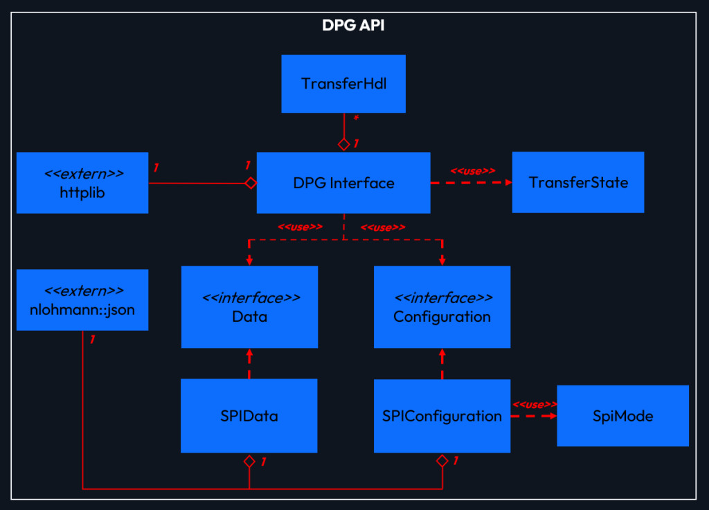
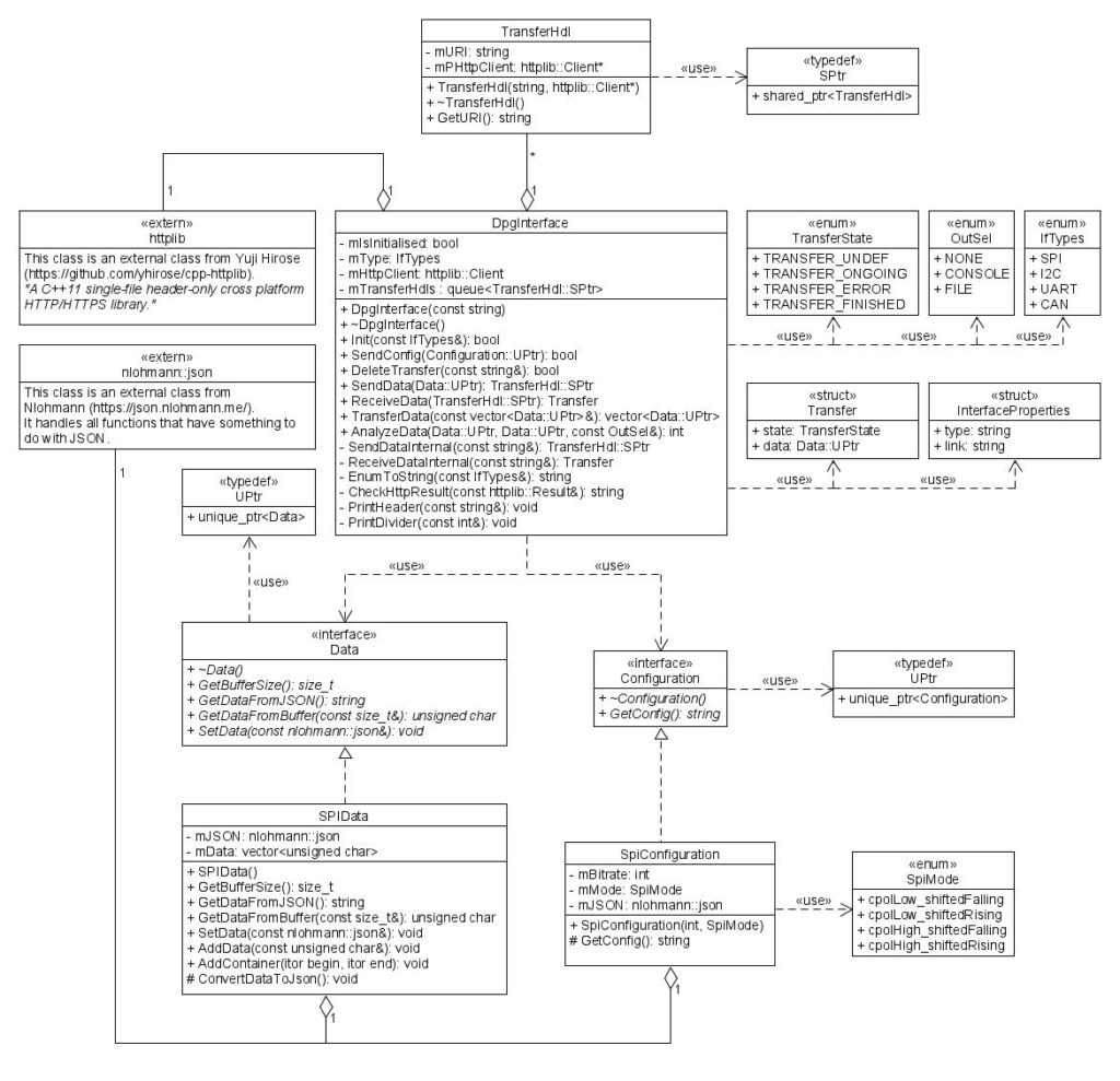
DPG API
- Enables the creation of data objects
- Sends and receives test data to the DPG
- Transfers a bunch of test data bundled together in a STL-container
- Analyses/compares the received data with expected data
- Integratable in existing test automation environments
- Written in C++ (ISO C++ 14 Standard)
This API library offers the user a variety of functions to work and communicate with the DPG.
It is written in ISO C++ 14 Standard and can be integrated in an existing test environment.
The user is provided with the file “Dpg_Api.lib” and all necessary header files.
These must be integrated into the respective development environment.
The following settings only applies to Microsoft Visual Studio Enterprise 2019:
In order to use the library, the user must include the file “DPG_Api.lib” in the solution properties.
To do this, the path to the file must be entered under “VC++ Directories –> Include Directories”.
Furthermore, the file must be entered under “Linker –> Input –> Additional Dependencies”.
After these settings have been made and the header files have been included in the solution, they can
be used in the user’s programme by means of “include”.
When declaring a DpgInterface object, a URL with the following appearance must be passed:
- URL = “IP-address:port” (The port is usually “8080”!)
- Examples:
- DpgInterface dpg(“192.168.172.15:8080”);
- DpgInterface dpg(“localhost:8080”);
- DpgInterface dpg(“10.24.99.2:8080”);
After the DpgInterface object has been declared, the functions can be accessed.
Each function has an appropriate return value to check for correct execution.
The first important function is “Init()”. This function must always be the first to be executed.
Subsequently, the function “SendConfig()” should be called/used.
After this, the functions for sending, receiving and analysing data can be executed as often as desired.
All calls should be in a try-catch block, as the external libraries “json.hpp” and “httplib.h” throw an
exception in the event of an error.
The HPS System
- Dual core ARM Cortex A9
- Bridges to communicate with the FPGA fabric
- 1 GiB of DDR3 memory
- Runs a Linux kernel and Uboot.
- Linux is built with buildroot
- Linux Kernel v.5.4 + busybox
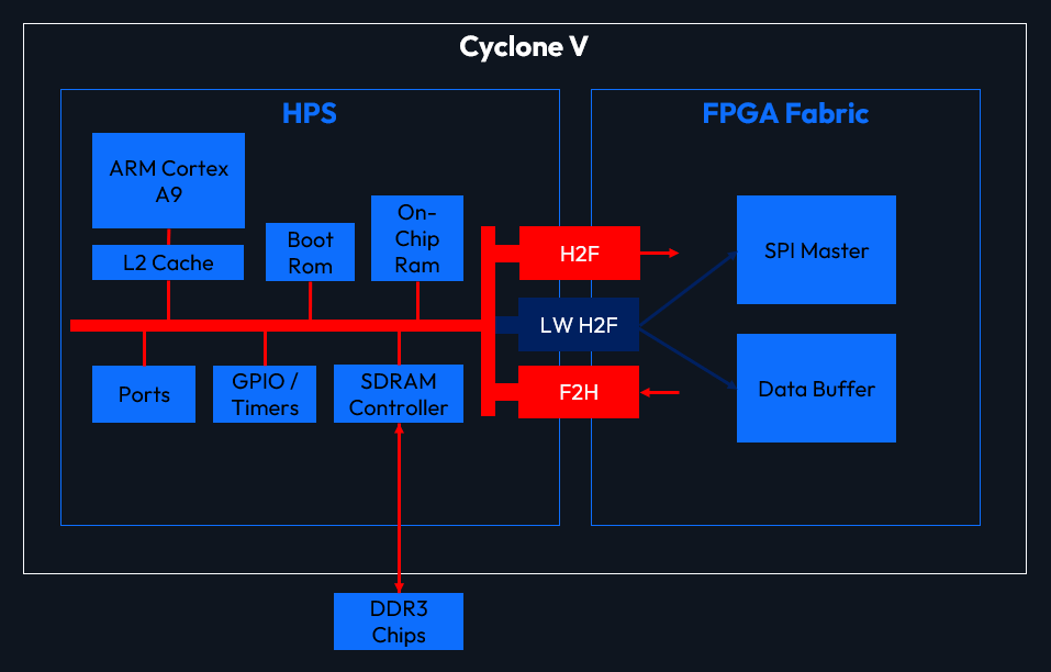
The CycloneV SoC includes a Hard Processor System (HPS) with a dual-core ARM Cortex A-9 CPU.
The HPS can communicate with hardware components in the FPGA over fast Bridges and is connected to 1 GiB of DDR3 memory.
It can run a mainline Linux kernel and Uboot, which makes it possible to use an up-to-date Linux based system.
Our Linux system is built with buildroot and uses a Linux Kernel with version 5.4 and busybox.
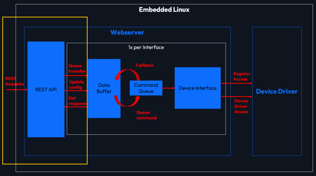
REST API
- Sends & receives data from the DPG API
- Forwards the data to the software queues
- Updates the configuration of the ip cores
- Checks the states of the hardware interfaces
- Easily extendable to support additional hardware components
- Written in Rust
Running on the Linux system is a webserver, that provides a REST-API for using the DPG over the local network.
The API supports sendins and receiving data, as well as updating the configuration and checking the status of each hardware interface.
Its discoverability makes it possible to write generic clients that can expose different options based on the connected device.
Although it runs only a single SPI master right now, the server is designed to be extensible and support multiple different hardware components simultaneously.
Queue & Driver Interface
- One queue for every component
- Buffers data until the hardware is ready
- Ensures that all requests are processed in the correct order
- Uses the linux device drivers to access the hardware
- Written in Rust
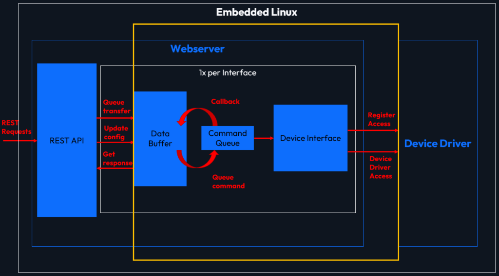
Additionally, the server has a queue for each component, that buffers data transfers until the hardware is ready.
The buffering still guarantees, that all data transfers and configuration updates are completed in the correct order as they appear on one interface.
The server includes a demo-mode, that can be run on any PC. The demo-mode can be used to debug or test a client that needs to communicate with the DPG later.
Linux Device Driver
- Data transfer with character device
- Setting and reading configuration values with sysfs
- Only one user access (mutex locked)
- No data loss due data buffering with a FIFO
(Read can be performed asynchronous) - Written in C
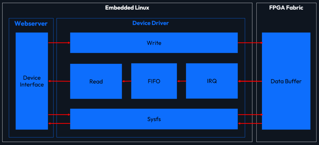
The driver makes communication between the HPS and the FPGA possible.
A open and release function is provided, these two functions use a mutex for locking the file access, so only one user has access at a time.
A character device is used for transferring data between the webserver and the data buffer, for this task write and read functions are provided.
The write and read function can be accessed in: /dev/spi_master
The data for the write function should be provided in binary format and it is possible to send uneven amount of bytes, the same format is used when the data is provided in the read function.
When data is written with the write function a wait queue is used to ensure that the buffer level of the data buffer is not violated (Each write increases the buffer level).
After writing the data, the data buffer gets the signal that it can start the transfer and when its done and interrupt is triggered.
In the interrupt routine the data is saved in a kfifo, the buffer level is decreased and the wait queues get a wake up signal.
Now it is possible to use the read function to get the data back to the HPS, the read function also uses a wait queue to ensure that data is available when the read is performed.
This workflow ensures, that no data get lost and the data can be read asynchronous.
For setting or reading the configuration values of the SPI master sysfs files are used.
The git revision is read only but read and write support is provided for CPOL, CPHA, pre delay, post delay and clock per half bit.
The sysfs files can be accessed in this path: /sys/bus/platform/drivers/dpg_spi_master
Data Buffer
- Soft IP Core (in FPGA Fabric)
- Double Buffer
- Buffers all data for the SPI Master
- Configurable via a memory mapped Interface
- Interrupt-Functionality
- Written in VHDL
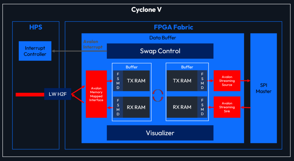
The “Data Buffer” is an ip core located in the FPGA fabric. The main task is to receive data coming from the software and store it until the SPI Master requests it. This allows a much higher clock frequency, because it is not depended on the SPI frequency.
Therefore four block rams (M10K) are used. Two rams are for sending the data from the driver to the SPI Master. They are called the “TX RAMs”. The other two rams are for receiving the data from the SPI Master, which are called “RX RAMs”. All ram blocks are mixed width dual port rams. This means that the software can send and receive 32 Bit always. On the other side, the transfer to/from the SPI Master is in bytes always.
The driver can interact with the buffer over a memory mapped interface based on “Avalon Memory Mapped”. There it can write data, read data or set some controls like starting a transfer or activating the interrupt.
Logical there are two buffers. Every buffer consists of one TX RAM and one RX RAM. The buffer can be swapped during the operation, to store upcoming data, while the current data is transmitted.
The buffer swap is done via the “Swap Control”. The “Swap Control” checks the state of the buffers finite state machines (every buffer has four – two for the storing and sending the data to/from the “TX RAM”. Two for sending and storing the data to/from the “RX RAM”) regularly. If the drivers initiates a swap by setting the bit over the memory mapped interface, the “Swap Control” will swap the buffers, if every state machine is finished.
The transfer to SPI Master is done via two “Avalon Streaming” interfaces. One functions as source, the other as sink. The source waits on the backpressure signal coming from the SPI Master. It sends all data stored in the ram byte for byte. In the meantime, the sinks receives the same amount of data and stored it in the “RX RAM”.
Device drivers can use the interrupt functionality of the Data Buffer. Therefore they need to activate the interrupt over the memory mapped interface. When activated, the Data Buffer initiates a interrupt whenever all data is received (coming from the SPI Master).
SPI Master
- Soft IP Core (in FGPA Fabric)
- Generates SPI Signals
- Bidirectional communication
- Receives data from the data buffer
- Configurable via a memory mapped Interface
- Written in VHDL
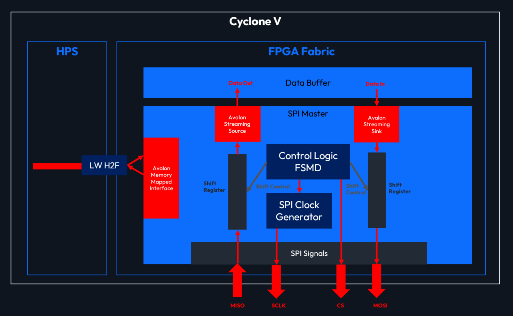
The spi signals that we want to transfer will be generated by a separate ip-core (SPI Master). This ip-core has interfaces to exchange data with the data buffer and to be configured by the HPS. For this purpose standard interfaces (avalon) were used to make the component as independent as possible.
The configuration of the ip-core is accomplished via an “Avalon Memory Mapped” interface.
Here we can configure settings such as:
- CPOL (Clock Polarity)
=> address offset 0x0 - CPHA (Clock Phase)
=> address offset 0x1 - Pre Delay (CS to SCLK) in Clock Cycles
=> address offset 0x2 - Post Delay (SCLK to CS) in Clock Cycles
=> address offset 0x3 - SCLK speed in Clock Cycles per half SCLK
=> address offset 0x4
The data that will be send or received via the SPI interface can exchanged with the data buffer over an “Avalon Streaming” interface. More specifically the ip core has a sink for receiving data and a source for sending data. Both interfaces work separate from each other and will send 8 bits of data as one package.
The spi signals generated by the ip core can be accessed using the standard SPI interface:
- MOSI (Data-Output)
- MISO (Data-Input)
- SCLK (SPI-Clock)
- CS (Chip-Select, active low)